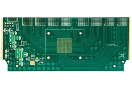
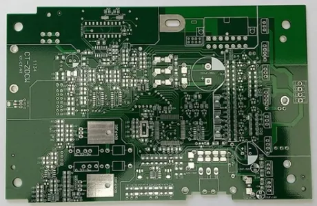
4-layer Spray Tin FR4 Communication PCB Circuit Board
Description :
4-layer spray tin FR4 communication PCB circuit board is a type of PCB specially designed for communication applications. It is optimized for transmitting and receiving signals, ensuring reliable and efficient communication between electronic components.Product Details:
4-layer Spray Tin FR4 Communication PCB Circuit Board Introduction
4-layer spray tin FR4 communication PCB circuit board is a type of printed circuit board (PCB) that is specially applied in communication devices. It uses FR-4 material as the primary insulating backbone and has four layers of conductive traces and insulating material. The spray tin surface finish provides protection and facilitates soldering.
4-layer Spray Tin FR4 Communication PCB Circuit Board Parameter
| Number of layers | 4 |
| Substrate | FR4 |
| Thickness | 1.6mm |
| Surface Treatment | Lead spray tin |
| Special Process | Impedance |
| Minimum aperture | 0.3mm |
| Inner layer line width and line spacing | 11/6mil |
| Outer layer line width and line spacing | 11/5mil |
| Applications | Mainly used in Wireless integrated access equipment |
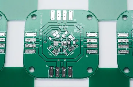
4-layer Spray Tin FR4 Communication PCB Circuit Board Features
The 4-layer spray tin FR4 communication PCB circuit board has several features that make it suitable for communication applications. Here are some key features:
1. FR4 Material: The PCB is made using FR4 material as the primary insulating backbone. FR4 is a widely used substrate material for PCBs due to its low cost, good resistance-weight ratio, excellent flame retardance, high mechanical strength, and good insulating capacity in dry or humid environments.
2. 4-layer Design: The PCB has four layers of conductive traces and insulating material. The additional layers allow for more routing options and can help reduce electromagnetic interference (EMI) and crosstalk between traces. These all can improve the signal integrity in communication applications.
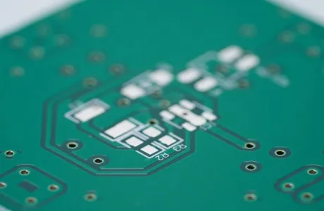
3. Spray Tin Surface Finish: The PCB has a spray tin surface finish. This involves applying a layer of tin on the surface of the PCB. The spray tin surface finish helps protect the copper traces and pads from oxidation and provides a solderable surface for components to be soldered onto the PCB.
4. Copper Foil Layers: The PCB is laminated with one or more layers of copper foil using heat and adhesive. These copper layers form the circuits in the finished product and may cover one or both sides of the PCB, depending on the design.
5. Cost-effective: FR4 material is widely available and relatively inexpensive compared to other substrate materials, making it a cost-effective option for PCB manufacturing.
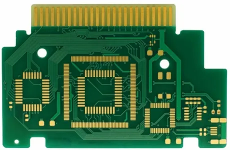
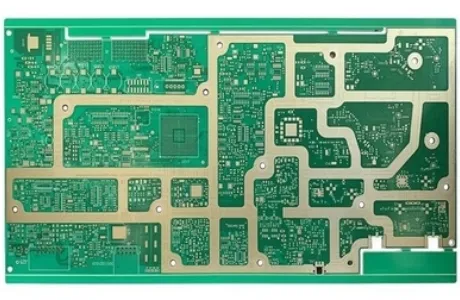
4-layer Spray Tin FR4 Communication PCB Circuit Board Applications
As the name suggests, these PCBs are specifically designed for communication systems. They are widely used in devices such as routers, switches, modems, wireless communication modules, and telecommunication equipment.