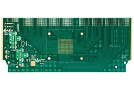
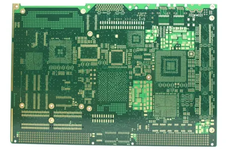
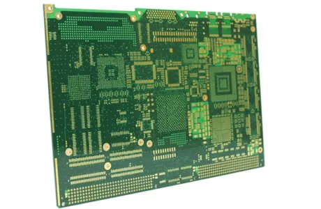
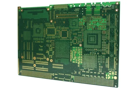
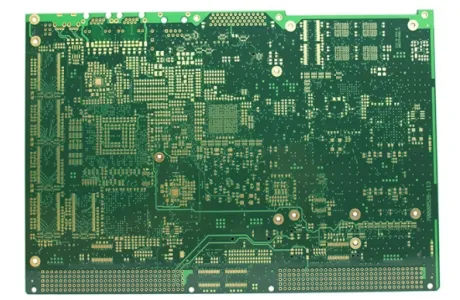
14-layer Immersion Gold Blind & Buried Via Industrial Control Equipment Motherboard
Description :
14-layer immersion gold blind & buried via industrial control equipment motherboard is a type of printed circuit board (PCB) specially used in industrial control equipment. Blind and buried vias are a special process used in the PCB (Printed Circuit Board) manufacturing process. Its main feature is to drill holes directly on the pads and then insert the components into the holes, thus enabling quick assembly of the circuit board. This technology can greatly simplify the PCB assembly process and improve production efficiency. Compared with traditional through-hole insertion technology, blind and buried via circuit boards have higher reliability and lower cost, which is expected to continue to play an important role in future development.Product Details:
14-layer Immersion Gold Blind & Buried Via Industrial Control Equipment Motherboard Introduction
14-layer immersion gold blind & buried via industrial control equipment motherboard is a type of printed circuit board (PCB) specially used in industrial control equipment. It has 14 layers and uses immersion gold as the surface finish. The board also features blind and buried vias, which are used to connect different layers of the PCB. The blind vias connect the outer layer with at least one inner layer, while the buried vias are located between two or more inner layers and are not visible from the outer layers.
14-layer Immersion Gold Blind & Buried Via Industrial Control Equipment Motherboard Parameter
| Number of layers | 14 |
| Substrate | FR4 |
| Thickness | 1.6mm |
| Surface Treatment | Immersion Gold |
| Special Process | Blind and buried vias |
| Minimum aperture | 0.2mm |
| Inner layer line width and line spacing | 4/3.5mil |
| Outer layer line width and line spacing | 4/5mil |
| Applications | specifically designed for industrial control systems like industrial control equipment motherboard |
14-layer Immersion Gold Blind & Buried Via Industrial Control Equipment Motherboard Features
1. High Density
The use of blind and buried vias allows for a higher density of circuitry on the motherboard. This means more components can be packed into a smaller space, making it suitable for applications with limited space requirements.
2. Improved Signal Integrity
The use of blind and buried vias helps to minimize signal interference and crosstalk between different layers of the PCB. This leads to improved signal integrity and reduced noise, ensuring the reliable performance of the industrial control equipment.
3. Enhanced Reliability
The immersion gold surface finish provides excellent corrosion resistance and solderability, ensuring the long-term reliability of the motherboard. Blind and buried vias can not only avoid problems such as pin bending and short circuits that may occur during through-hole insertion but also have strong resistance to vibration and impact, making it suitable for various harsh environmental conditions.
4. Optimize PCB Wiring Design
The application of blind via and buried via technology can help optimize PCB wiring design and improve circuit performance and reliability.
5. Reduce PCB Manufacturing Costs
The application of blind via and buried via technology can also reduce PCB manufacturing costs, such as reducing material usage, improving production efficiency, and reducing maintenance costs.
6. Easy Operation
The operation process of blind and buried vias is relatively simple. You only need to drill holes in the pads and then insert the components into the holes. This greatly reduces the operating difficulty and skill requirements of workers.
7. Enhance the Flexibility of PCB Design
It can be embodied in the following three aspects:
- Support different design styles: The application of blind via and buried via technology makes PCB design more flexible and changeable. According to different needs and application scenarios, designers can choose different design styles to meet customers' customized needs.
- Enhanced repairability: By using blind and buried via technology, certain components can be repaired or replaced without damaging the PCB. This greatly improves PCB repairability and reduces repair costs and time.
- Improve adaptability: Blind hole and buried hole technology can make PCB better adapt to different working environments and conditions. For example, in limited space or harsh environments, PCBs using blind via and buried via technology can better leverage their performance advantages.
14-layer Immersion Gold Blind & Buried Via Industrial Control Equipment Motherboard Applications
Blind and buried via circuit boards, including 14-layer immersion gold blind & buried via industrial control equipment motherboard, can achieve higher circuit density and smaller size, thereby improving the performance and reliability of industrial control systems. They are largely used in programmable logic controllers (PLCs), automation systems, robotics, etc.
Frequently Asked Questions about Blind and Buried Vias
1. What Exactly are Blind and Buried Vias?
A blind Vias connects the outer layer to one or more inner layers but doesn’t go through your whole PCB.
A buried vias connects two or more inner layers, but won’t go through to the outer layer. It is buried within the circuit and completely internal. So it is not visible to the naked eye.
2. What Are Blind and Buried Vias Advantages?
Blind and buried vias can help you meet the high-density constraints of lines and pads on a typical design without increasing the overall layer count or your board size. The vias also help you manage the printed circuit board aspect ratio and limit the change of break out.
3. What Are Blind and Buried Vias Disadvantages?
Cost is still the main issue with boards using blind and buried vias, compared to the boards using standard through-hole vias. The high cost is due to the increasing complexity of the board and more steps in the manufacturing process. At the same time, testing and precision checks are made more frequently.
4. Why Do Blind and Buried Vias Emerge in the PCB Manufacturing Industry?
This answer should start from a traditional multilayer printed circuit board. The structure of the standard multilayer PCB has outer layers and inner layers, to achieve the inner connection function between every circuit layer, you should use plated through via holes and make the vias metallization. But you know the size of the printed circuit is limited, so if you want to achieve more function and put more high-performance parts in the board in PCB assembly, you have to add more circuit lines to the board.
Except for making thinner circuit line width, the DIP plug-in via size zooms out from 1 mm to SMD 0.6 mm and further zooms out below 0.4 mm. But it still will occupy the surface area of PCB, so blind and buried vias emerge in a few high-tech PCB board manufacturers as the times require.